

ACCELERATE PCB PROTOTYPING IN YOUR LAB
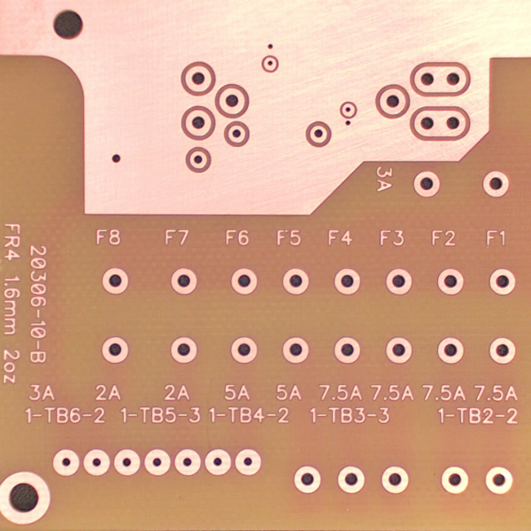
- From Gerber data to a physical prototype in-house – reduce dependency on external prototype manufacturing cycles.
- No chemical etching process – mechanical PCB fabrication without the chemical etching stage.
- End-to-end in-house workflow – milling, drilling, through-hole connection, solder paste, component placement and reflow.
FROM GERBER FILE TO FINISHED PCB
Complete in-house workflow for PCB prototyping, from manufacturing data preparation and milling to component placement and reflow.
CAM & DATA PREP
Prepare Gerber and Excellon manufacturing data, create machining operations and review toolpaths with TrackMaker. →
MILLING & DRILLING
Create PCB isolation paths, drill holes and machine the final board contour using 4MILL CNC systems. →
THROUGH-HOLE CONNECTION
Create mechanical electrical connections between the two sides of double-sided prototype PCBs using conductive rivets. →
SOLDER PASTE APPLICATION
Apply solder paste using stencil printing or pneumatic dispensing according to the PCB and assembly requirements. →
COMPONENT PLACEMENT
Position SMD components manually with vacuum pickup, visual assistance and optional component feeders. →
SOLDERING & REFLOW
Reflow the assembled PCB using a controlled thermal process selected for the solder paste and board assembly. →
WHAT MAKES MIPEC DIFFERENT
FROM PCB MILLING TO A COMPLETE SMT WORKFLOW
Start with PCB milling and expand the laboratory workflow step by step into solder paste application, component placement and reflow as requirements grow.
TRACKMAKER PCB CAM SOFTWARE
PCB-focused CAM software for preparing Gerber and Excellon manufacturing data, creating machining operations and preparing projects for 4MILL milling and drilling.
SINGLE-SOURCE HARDWARE SUPPORT
MIPEC supplies the core PCB prototyping equipment together with compatible tooling, extraction systems, accessories and technical support for the complete laboratory workflow.
I would like to thank you very much for taking part in the project. It was a great benefit for me personally. Even when things had to be solved quickly and adjusted along the way, from my point of view everything was always handled perfectly. I really appreciate the excellent communication, and I would be very happy to work together again in the future.
TEST YOUR PCB DESIGN WITH MIPEC
Want to see how your own PCB design performs with mechanical milling? Send us your Gerber and Excellon data by email. We will review your files, manufacture a sample PCB using MIPEC equipment and send the finished board to you free of charge.